
They are already here. The leaks of the last days invited us to suspect that the first processor of the Apple M2 family could see the light during this edition of the WWDC (Worldwide Developers Conference), and finally it has been so. The first devices to integrate this chip will be the redesigned MacBook Air and the 13-inch MacBook Pro, but there is no doubt that in the coming months will come to other proposals of this brand.
Apple does not usually reveal the deepest details about the microarchitecture of its processors (in this field, Intel and AMD do tend to appease the appetite of enthusiasts who like to investigate their proposals). Even so, during the presentation of the M2 chips, those from Cupertino have given us the information we need to form an accurate idea about what does it promise us this CPU.
googletag.cmd.push(function() { googletag.display(“div-gpt-out”); });
And what it promises us, very roughly, is more power and a higher performance/watt ratio than that delivered by the M1 microprocessor. However, this is not all. The information we have about this chip allows us to guess what the processors will offer us M2 Pro, M2 Max and M2 Ultra when they arrive. And they will come. Of that we can be sure. This is how the new Apple microprocessor spends them.
Apple’s M2 processor in numbers
|
M2 |
M1 |
|
|---|---|---|
|
photolithography |
5nm (2nd generation) |
5nm |
|
number of transistors |
20 billion |
16 billion |
|
maker |
TSMC |
TSMC |
|
number of cpu cores |
8 |
8 |
|
high performance (ar) cores |
4 |
4 |
|
high efficiency cores (ae) |
4 |
4 |
|
CACHE INSTRUCTIONS (AR) |
192KB |
192KB |
|
DATA CACHE (AR) |
128KB |
128KB |
|
CACHE INSTRUCTIONS (AE) |
128KB |
128KB |
|
DATA CACHE (AE) |
64KB |
64KB |
|
shared l2 cache ar cores |
16MB |
12MB |
|
shared l2 cache ae cores |
4MB |
4MB |
|
number of graphics cores |
10 |
8 |
|
fp32 performance |
3.6 TFLOPS |
2.6 TFLOPS |
|
NEURAL ENGINE NUCLEI (NE) |
16 |
16 |
|
performance logic ne |
15.8 TOPS |
11 tops |
|
maximum unified memory map |
24GB |
16 GB |
|
main memory technology |
LPDDR5-6400 |
LPDDR4X-4266 |
|
unified memory bandwidth |
100GB/s |
68GB/s |
|
video encoding and decoding |
8K H.264, H.265, ProRes and ProRes RAW |
4K H.264 and H.265 |
|
connectivity |
2 x Thunderbolt 3/USB 4 |
2 x Thunderbolt 3/USB 4 |
M2 chip microarchitecture improvements show promise
Unfortunately, the information that Apple has revealed about the improvements that it has implemented in the microarchitecture of the M2 processor it’s not that deep as we would have liked. We do not know what innovations it has introduced in the execution pipeline, how the new code branch prediction algorithms work or what the management policy of the different cache memory sublevels is like, among other particularities of each microarchitecture.
Still, we have the information we need to connect some important dots. Lets start by the beginning. We know that the M2 processor is being manufactured by TSMC on its 5nm node, but it is not the same photolithographic equipment on which this Taiwanese company is producing the M1 chips, which also use 5nm integration technology; the M2 microprocessor is being manufactured using second generation 5nm photolithography. The pity is that everything, but as soon as we know them we will investigate them in a new article.
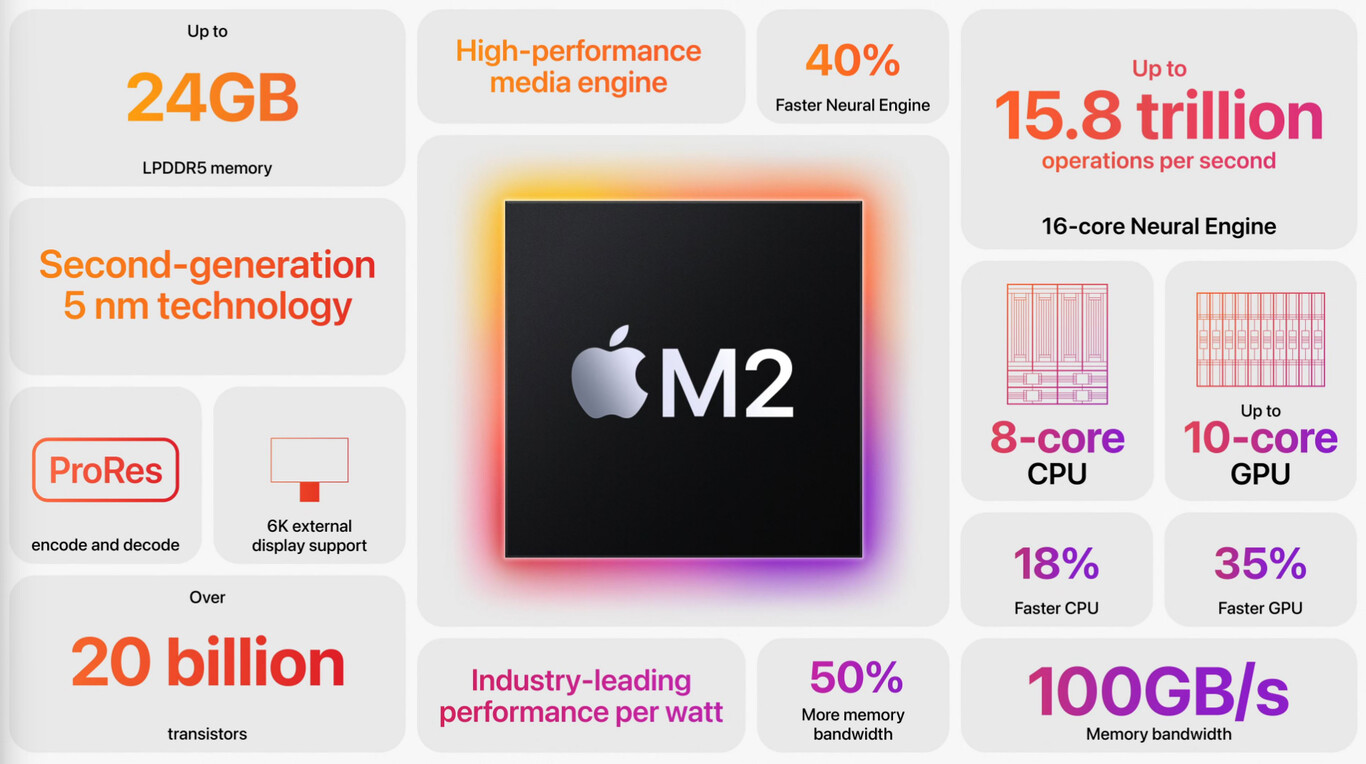
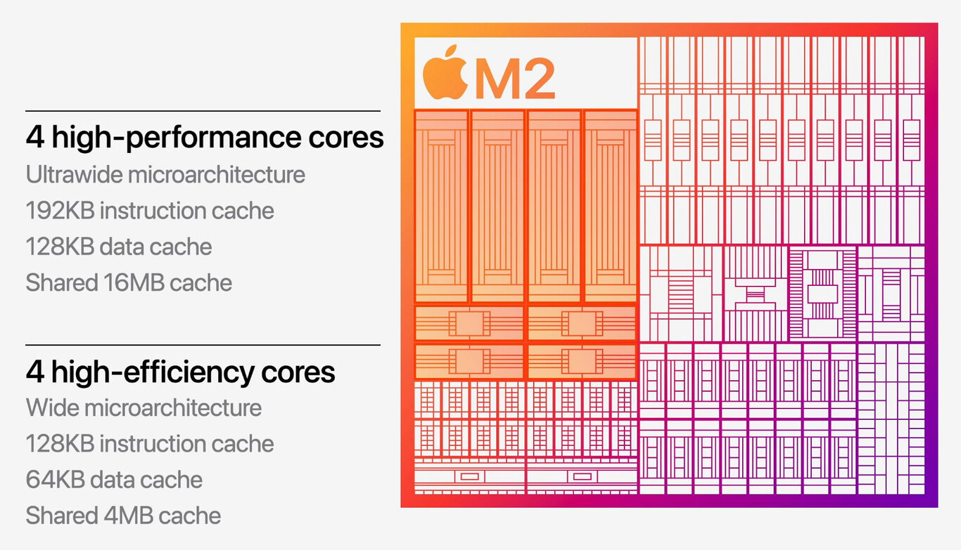
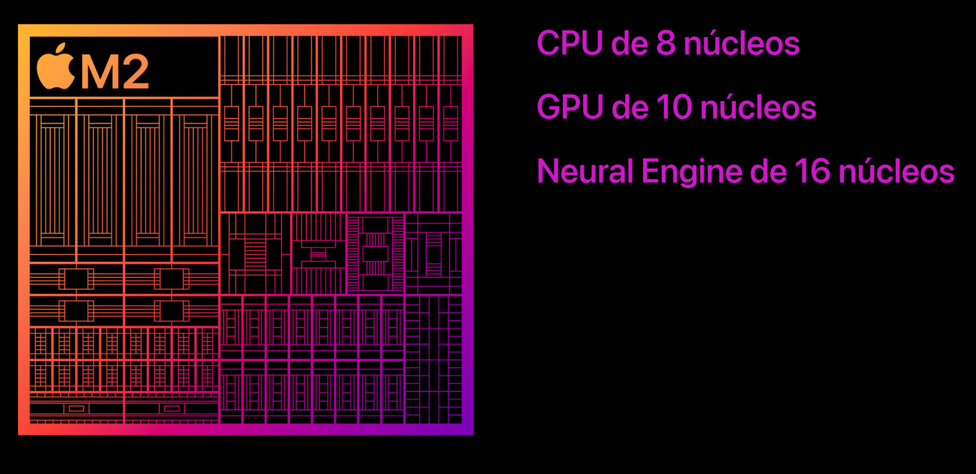
Another interesting fact: the M2 processor brings together 20 billion transistors, while the M1 incorporates 16,000 million. The 4 billion additional transistors respond, as we can guess, to the modifications that Apple engineers have introduced in the microarchitecture. Of course, both chips incorporate the same number of CPU cores: 4 high-performance (AR) and another 4 high-efficiency (AE).
It is very reasonable to expect that the management policy of the different cache sublevels, and perhaps also their latency, will be different in the M1 and M2 chips.
The instruction and data caches linked to the AR and AE cores are the same size on the M2 and M1 chips (we indicate their capacity in the specification table above). On the other hand, the AE cores in both processors access a shared level 2 cache memory with a capacity of 4 MB, but, and here the M2 chip differs from the M1, the AR cores in the new Apple processor have at their disposal reach a level 2 shared cache with a capacity of 16MBwhile in the M1 chip this figure is reduced to 12 MB.
As we have just seen, only the shared level 2 cache accessed by the high-performance cores has increased in capacity in the M2 processor, but this does not mean that this is the only difference that Apple has introduced in the cache subsystem. . It is quite reasonable to expect that the management policy of the various cache sublevels, and perhaps also their latency, are different in the M1 and M2 chips. The latter on paper should be helped by the improvements that Apple engineers have introduced.
The scope of the news is not limited only to the general purpose cores of the M2 processor; The graphic logic has also been redesigned, although for the moment Apple has hardly revealed details that allow us to intuit the magnitude of the changes that it has implemented in the integrated GPU. What we do know is that the M2 chip incorporates 10 graphics cores (two more than the M1 processor), and also that its performance in single precision floating point operations (FP32) is 3.6 TFLOPS, which allows it to lead the M1 chip by 1 TFLOP.
The artificial intelligence engine of the M2 chip is capable of carrying out 15.8 trillion operations per second
With the artificial intelligence engine implemented in these microprocessors, essentially the same thing happens. We do not know in detail how the Neural Engine logic of the M2 and M1 chips differs, but Apple has confirmed that both have the same number of cores: 16. Of course, they are not the same. And we know that they are not because the AI engine of the M2 chip is capable of carrying out 15.8 trillion operations per second, while that of the M1 is close to 11 billion operations per second. In both cases it is about billions of us, not the Anglo-Saxons.
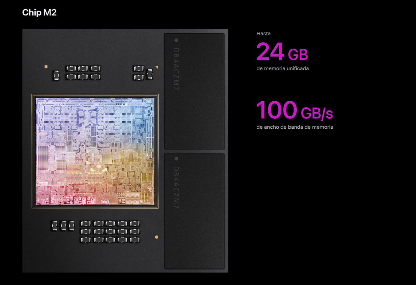
Before going any further it is worth looking into the features of the M2 processor’s unified main memory. Unlike the M1 chip, which can ‘only’ live with 16GB of memory, the M2 can access a 24GB unified map. In addition, this memory is in the new Apple chip of the LPDDR5-6400 type, while in the M1 processor it uses the LPDDR4X-4266 technology. This modification, and this data is very important, allows the interface of the unified memory of the M2 to reach a bandwidth of up to 100GB/swhile the memory interface of the M1 settles for a more restrained 68 GB/s.
We have already delved into the most relevant elements of the M2 processor logic, but before moving on to the next section of the article it is worth taking a look at another area where, on paper, Apple has done its homework: the video encoding standards that your new processor can deal with. According to those from Cupertino, its M2 chip can play content with a maximum resolution of 8K encoded in the formats H.264, H.265, ProRes and ProRes RAWwhile the M1 processor is capable of handling 4K UHD H.264 and H.265 content.
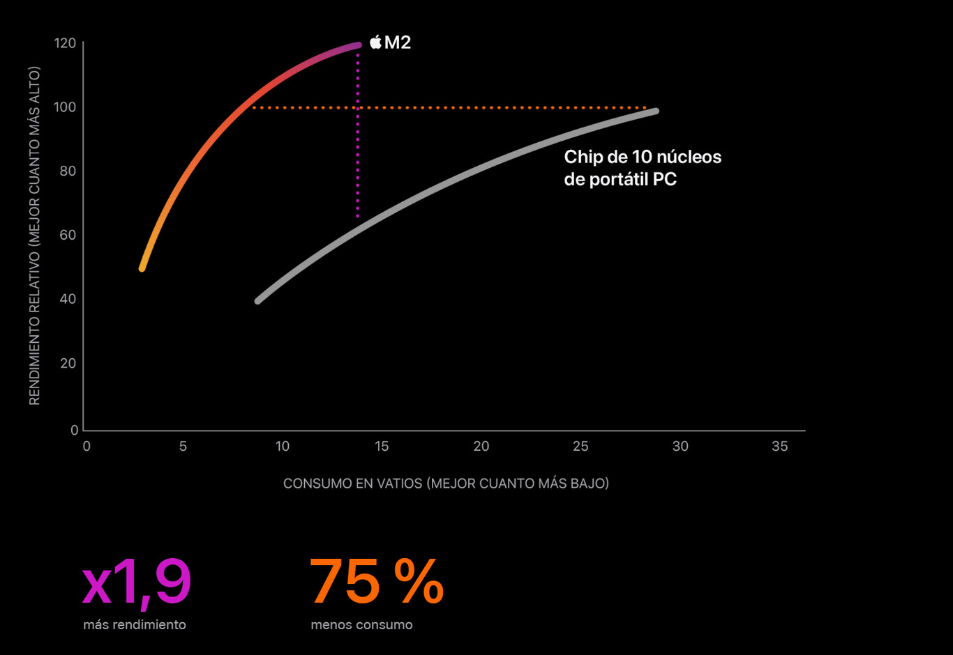
This is how the M2 processor performs (according to Apple)
On the next slide we can see that, according to Apple, the M2 microprocessor built into the new MacBook Pro almost doubles the performance of a Samsung Galaxy Book2 360 laptop equipped with an Intel Core i7-1255U CPU and 16 GB of RAM when both draw just under 15 watts.
And at the same consumption, the Cupertino chip always delivers a clearly higher performance than that of the Intel processor. When we have the opportunity to analyze the first Apple computer equipped with an M2 processor that falls into our hands, we will see if, indeed, your performance per watt it is as attractive as Apple defends.
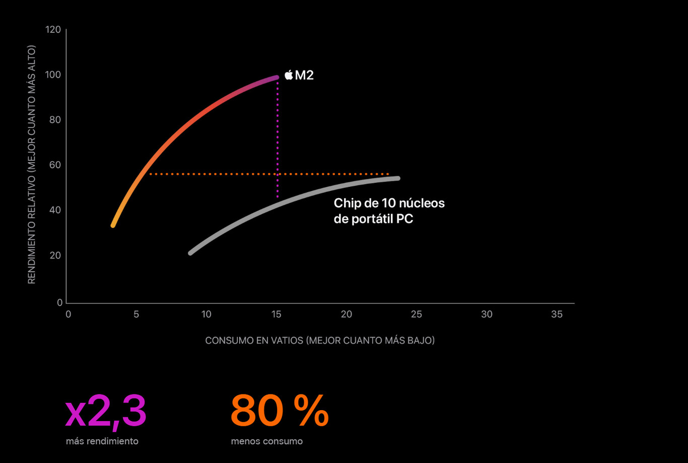
The following graph compares the performance of the new MacBook Pro equipped with an M2 processor and the same Samsung Galaxy Book2 360 equipped with an Intel Core i7‑1255U CPU and 16GB of RAM from the previous graph. The result? When both consume 15 watts the graphics logic integrated in the M2 chip multiply by 2.3 Intel processor graphics performance.
And when both graphic logics give us a relative performance slightly lower than 60, the M2 processor consume 80% less than the Intel chip. In any case, for the moment it is most prudent that we collect this data with some skepticism because Apple, as we all know, is an interested party. It will be very enlightening to see for ourselves whether the M2 processor really lives up to expectations when the first computer equipped with this chip falls into our hands.
(function() {
window._JS_MODULES = window._JS_MODULES || {};
var headElement = document.getElementsByTagName(‘head’)[0];
if (_JS_MODULES.instagram) {
var instagramScript = document.createElement(‘script’);
instagramScript.src=”https://platform.instagram.com/en_US/embeds.js”;
instagramScript.async = true;
instagramScript.defer = true;
headElement.appendChild(instagramScript);
}
})();


