
the machines of extreme ultraviolet photolithography (UVE) manufactured by the Dutch company ASML are a marvel of technology. In fact, without them the most advanced integrated circuits produced by the largest semiconductor manufacturers on the planet, including TSMC and Samsung, would not be possible.
Their complexity is such that to explain how they work in some depth, I would have to dedicate not one, but several very extensive articles to them. Ignacio Mártil, professor of electronics at the Complutense University of Madrid and an authority on semiconductors, offers us in one of his very interesting articles several figures that can help us understand what we are talking about.
Just one of ASML’s UVE lithography machines contains more than 100,000 parts, 3,000 wires, 40,000 bolts and no less than two kilometers of electrical connections. There it is. However, the hardware is only one of the ingredients in the recipe. The other, and also essential, is the embedded software who is responsible for directing and supervising the proper functioning of each of the lithography equipment.
ASML currently occupies a central position in the semiconductor industry, and its status is undoubtedly the result of the titanic effort that this European company has put into R&D over the years. However, as we can guess, She hasn’t walked this path alone. 90% of the components of its lithography machines come from other companies spread all over the planet. And the role of at least two of them is fundamental.
Cymer supplies ASML with the raw material needed for its lithography machines
This American company founded in 1986 is specialized in the manufacture of lasers and deep ultraviolet light sources (DUV) and extreme (UVE). It has had a very close relationship with ASML for many years; In fact, the role of light sources manufactured by Cymer in lithography machines is so relevant that in 2013 ASML bought this San Diego company with the purpose of investing in it to accelerate the development of technologies involved in lithography. UVE.
Cymer somehow provides ASML with the raw material its photolithography machines need. And that raw material is none other than ultraviolet light, which is responsible for transport geometric pattern described by the mask so that it can be transferred very precisely to the surface of the silicon wafer. As we will see in the next section of the article, the optical elements designed and produced by the German company ZEISS are also involved in this process.
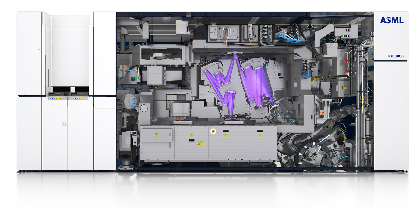
The most advanced photolithography equipment that ASML designs and manufactures is extraordinarily complex. The UV light source is housed in the bottom right-hand corner of the machine, and the wafers move through it with amazing precision.
Since we are involved in flour, it is worth investigating a little more about the characteristics of the light used by UVE lithography equipment. And its most striking property is that it belongs to the most energetic portion of the ultraviolet region of the electromagnetic spectrum. In fact, its wavelength extends in the range from 10 to 100 nanometers (nm).
UVE light must travel from the source to the silicon wafer without interacting with the slightest dust particle
The problem is that it is not at all easy to generate and deal with this form of electromagnetic radiation. And it is not, among other reasons, because it is so energetic that alter the structure of the physical elements with which it interacts inside the lithography machine.
In addition, the UVE light must travel from the source to the silicon wafer without interacting with the slightest dust particle, so it is necessary that the entire chip production process takes place inside a chamber designed to provide a high quality vacuum.
Fortunately, as we tell you in this article, a new procedure is being developed for vacuum measurement which will possibly make a difference in the lithographic processes that will arrive in the future.
ZEISS expertise in optics manufacturing is a safe bet for ASML
At the end of last year I had the opportunity to visit the ZEISS optics laboratory in the same building where he lives its headquarters, which is located in the German town of Oberkochen, just over 180 km from Munich. And I got a pleasant surprise.
I knew that this long-standing German company (it was founded in 1890) was involved in the production of optical elements for lithography equipment, but that visit helped me to more precisely identify the size of the optical equipment that ZEISS manufactures expressly for the UVE lithography machines that ASML produces.
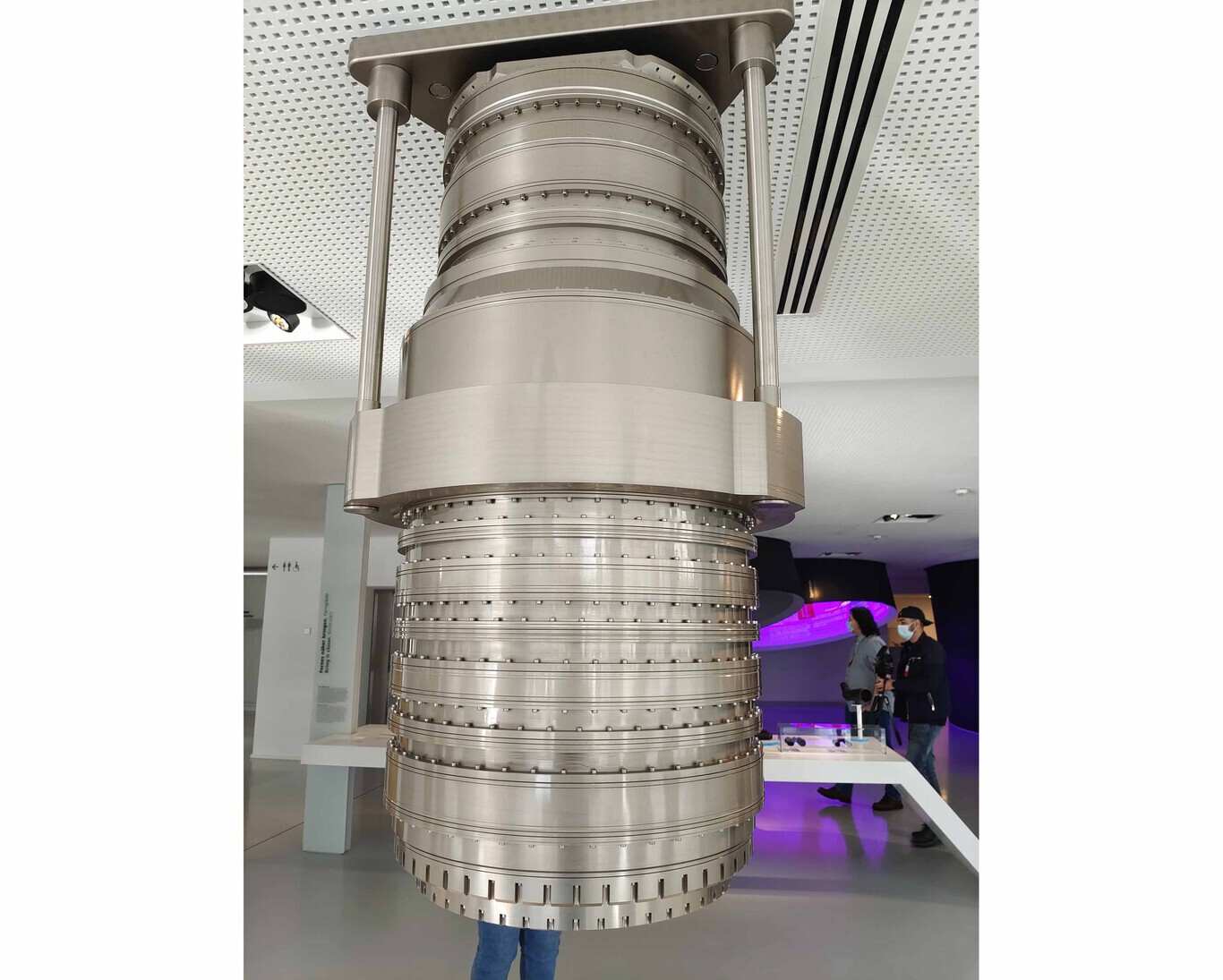
The lithography optic that we can see in this photograph is a Starlith 1700i manufactured by ZEISS. When you have it in front of you, its dimensions are intimidating.
The role of ZEISS optical elements in these lithography equipment is crucial. And it is because they take responsibility, leaving aside the most complex details, of transferring UVE light with a wavelength of 13.5nm from the source that is responsible for its emission to the mask that contains the geometric pattern that needs to be captured on the silicon wafer.
But this is not all. From this moment on, the projection optics come into action with the purpose of transferring the UVE radiation that already contains the geometric pattern to the wafer of semiconductor material. Put like that, it doesn’t seem very complex, but it is. It is a very complex process. If the mirrors involved in the propagation of UVE light are not manufactured with great precision, the geometric pattern defined by the mask will be altered, and the chips will go to waste.
In addition, the reflecting mirrors that are responsible for transporting the light from the emitting source to the mask must ensure that UVE radiation reaches the latter. with extreme uniformity. Otherwise, again, the IC manufacturing process will not be successful. However, ZEISS does not just produce the mirrors involved in this very delicate process.
It is also responsible for designing and manufacturing the sensors and actuators that are responsible for the work carried out by the optical equipment of the lithography machines. conforms to tolerances required by this process, which are extraordinarily restrictive. And to write the software that supervises in real time the correct functioning of this subsystem. There it is.
Images: ASML
| Ignatius Martil


