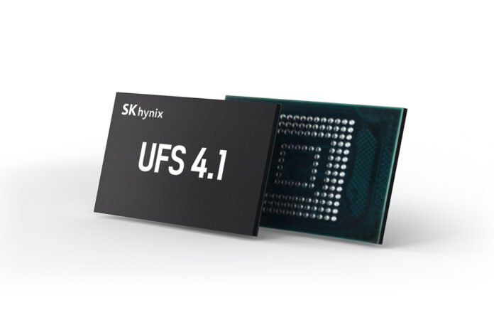
On-device artificial intelligence is about to receive a new, significant “boost” after the announcement of new increasingly performing components designed to equip the smartphones that will make their debut over the next few months and the next few years.
SK Hynix It is ready to take an important step forward, with the presentation of its new storage solution UFS 4.1 based on Nand a technology a 321 Layerthe highest in the world, which not only promises to raise the bar of performance for future flagship smartphones, but also launches a direct challenge to Samsung, one of the undisputed leaders in the memories sector.
Follow Samsung Italia on Telegram, Receive news and offers first
The new SK Hynix UFS 4.1 memories are a concentrate of speed and innovation at the service of AI
SK Hynix has officially announced the development of its UFS (Universal Flash Storage) 4.1 solution, which adopts the Nand Flash 4D Triple Level Cell (TLC) from 1 TB to 321 layerscurrently the most stratified in the world for mobile applications.
This milestone was designed specifically for the growing needs of on-device artificial intelligence (the one integrated in the device), where high performance and low energy consumption are fundamental for stable and reactive operation.
The specific They speak clearly: the new UFS 4.1 of SK Hynix reaches a sequential reading speed up to 4,300 MB/s. This is the highest sequential reading speed for a fourth generation UFS memory. But that’s not all, because the company also declares a significant improvement in the performance of random reading and writingrespectively of the 15% and 40% In addition to the previous generation.
The latter are crucial parameters for multitasking and general fluidity of the operating system and applications, especially when it comes to work related to AI.
The comparison with Samsung: a overtaking (marginal but significant)
In the competitive UFS memories market for smartphones, Samsung has long been a point of reference. Its UFS 4.0 solutions, used in top products, offer reading and writing speeds that reach 4,200 MB/if 2,800 MB/s respectively, based on a V-NAND building at 176 Layer.
With its 4,300 MB/s in sequential reading, the new UFS 4.1 of SK Hynix is therefore positioned marginally in front To the fastest solution currently offered by Samsung.
Although the difference in terms of MB/S may seem minimal, it is the technology underlying to mark an important step: i 321 Layer of Sk Hynix’s Nand against the 176 Layer of Samsung indicate a considerable progress in density and production sophistication.
Not only speed: energy efficiency and “Ultra-Slim” design efficiency
The news introduced by SK Hynix with its UFS 4.1 do not limit themselves to pure speed: in the official press release the South Korean company has also paid great attention to the energy efficiency and physical dimensions of the chip, increasingly crucial aspects in the design of modern smartphones, for example, think of devices such as the brand new Samsung Galaxy S25 Edge.
The new UFS 4.1 solution offers a 7% improvement in energy efficiency Compared to the previous generation of SK Hynix, based on NAND at 238 Layer. In the practical act, this means less battery consumption under the same performance, a detail not gradually for devices that have always been called to balance power and autonomy.
Compared to the past, the thickness of the new product has also been reduced: we talk about 0.15 mm lessreaching only 0.85 mm against the previous millimeter. This 15% reduction of the thickness is fundamental for integration in smartphones with a “ultra-sul” design, a trend that, as we mentioned previously, is increasingly widespread in the top of the range market.
As SK Hynix points out, even if these improvements may seem minor individually, in the extremely competitive market of smartphones every single bit of innovation counts.
In this regard Ahn HyunPresident and Chief Development Officer of SK Hynix, said the following:
We are on the right way to expand our position as a complete supplier of Memoirs AI in the NAND space by building a portfolio of products with a technological advantage AI.
The company, in fact, plans to complete the development of SSD based on the same Nand 4D technology at 321 layers, intended for both the consumer and data center market, also complete the development of SSDs.
Availability and new SK Hynix memories
SK Hynix plans to provide its new UFS 4.1 in two capacity cuts: 512 GB And 1 TB. As for the timing, the company aims to obtain the qualification by customers producing smartphones by the end of the current year and plans to start shipments in volumes starting from the first quarter of next year (then during Q1 2026).

