
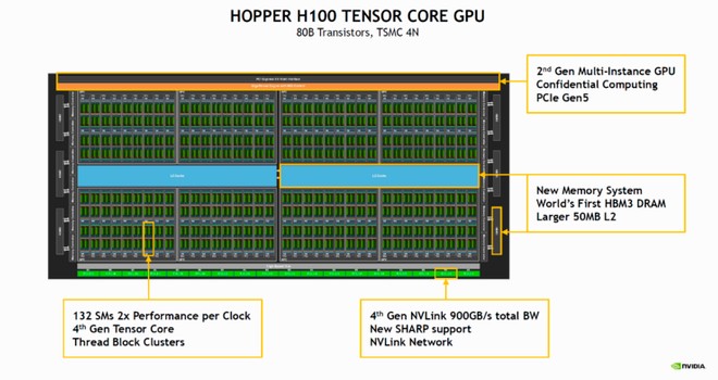
In March of this year, NVIDIA announced the Hopper H100 GPU as the successor to the Ampere A100. The hardware is geared towards data center applications and focuses on accelerating terabyte-scale workloads. For this, the component uses a new architecture with advanced mechanisms, such as the 4th generation of Tensor cores.
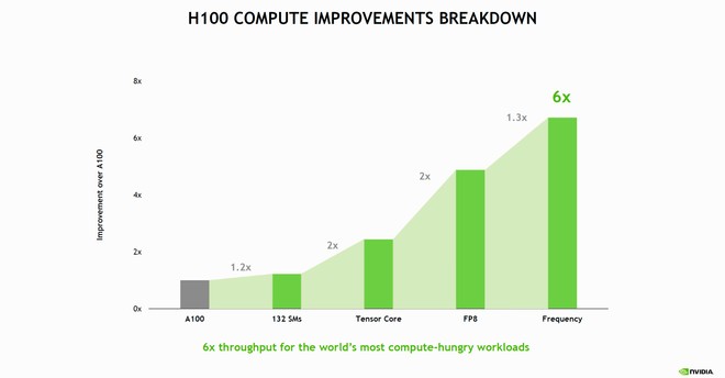
That’s what the company talked about at the conference Hot Chips 34 this Monday (22). The “green team” detailed the evolution of the new graphics chip during the virtual event, noting that the Hopper H100 GPU is capable of delivering data transfer rates up to six times higher than the Ampere A100 GPU.
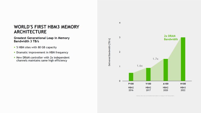
The H100 is produced using TSMC’s 4 nanometer (4N) process. This lithography opens the possibility for the GPU to work with 80 billion transistors, which optimize performance and efficiency. Another unique feature is the use of six layers of HBM3 RAM, such that they deliver up to twice the speed and capacity of up to 80 GB.
The platform has 8 clusters graphics processing cluster (Graphics Processing Cluster or GPC) that contain 9 clusters processing cluster (Texture Processing Cluster or TPC) — that is, it comprises a total of 72 TPCs. It is worth remembering that each TPC is composed of 2 stream multiprocessors (SMs), so the H100 has 144 SMs (18,432 CUDA).
This can be compared to the manufacturer’s current most advanced video card aimed at gamers. The GeForce RTX 3090 Ti, considered the most powerful in the world, is equipped with “only” 84 stream multiprocessors and are limited to the most affordable technologies, such as 4th generation PCI Express and 3rd generation Tensor cores.
And speaking of high-precision processing cores, used essentially in the GPU’s artificial intelligence tasks, the Hopper H100 uses the unprecedented 4th generation of Tensor cores. Compared to previous generation cores, these mechanisms are capable of delivering twice as much performance using the same clock frequency.
The Hopper H100 supports the FP8 format, allowing the hardware to work with high precision at 4,000 TFLOPs, plus 2,000 TFLOPs on FP16, 1,000 TFLOPs on TF32, and 60 TFLOPs on FP64. The numbers show that the Hopper H100 is 3.3 times faster than Ampere A100 and 28% faster than AMD Instinct MI250X at FP64.
The GPU will be made available to the server industry in two versions: one compatible with 5th generation PCI Express and one compatible with the SXM socket. The first has some limitations as it does not have full integration with the NVIDIA ecosystem, but it will still serve as a strong competitor to the successors of AMD’s Instinct MI200 GPU.


